PDF] Under Bump Metallurgy (UBM)-a technology review for flip chip packaging

By A Mystery Man Writer
Flip chip packaging technology has been utilized more than 40 years ago and it still experiencing an explosives growth. This growth is driven by the need for high performance, high volume, better reliability, smaller size and lower cost of electronic consumer products. Wafer bumping is unavoidable process in flip chip packaging, thus, picking the correct bumping technology that is capable of bumping silicon wafer at high yield and a high reliability with lower cost is challenging. This paper discusses the available wafer bumping technologies for flip chip packaging. The discussion will be focused on process assembly, solder ball compatibility, design structure and lastly cost which translated to overall product costs.

PDF) UNDER BUMP METALLURGY (UBM)-A TECHNOLOGY REVIEW FOR FLIP CHIP
UBM (OPM: Over Pad Metal, FSM: Front Side Metal and Electroless plating) Service - JX Metals
Cost, production, and logistics implications of C4NP solder bumping. - Document - Gale Academic OneFile

PDF) Under bump metallurgy (UBM) - A technology review for flip

PDF] Under Bump Metallurgy (UBM)-a technology review for flip chip packaging
Artificial intelligence deep learning for 3D IC reliability prediction

PDF) Under bump metallurgy (UBM) - A technology review for flip
Flip-Chip Interconnections: Past, Present, and Future

EHP_PhD-Thesis

A new failure mechanism of electromigration by surface diffusion of Sn on Ni and Cu metallization in microbumps

Flipchip bonding.

PDF) Under bump metallurgy (UBM) - A technology review for flip

Challenges Grow For Creating Smaller Bumps For Flip Chips

PDF) Under bump metallurgy (UBM) - A technology review for flip

Flip Chip Technology Versus FOWLP
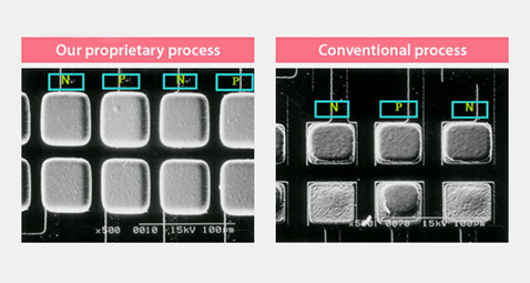
- Figure 3 from Under Bump Metallurgy (UBM)-a technology review for flip chip packaging

- My dog has bumps under her fur. What is the cause and treatment?
- Under Bump Briefs Storm in a D Cup Canada

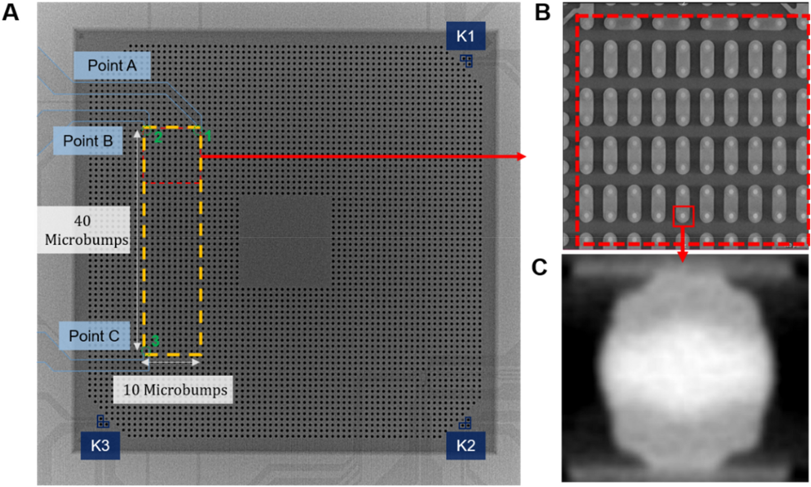
- a) Under-bump metallization and micro-bumps fabricated on the VLSI

- BumpStart Under Belly Maternity Leggings (2 Pack)- Black/Grey

- Stretch Vinyl Bright Hot Pink Flare Leggings High Waisted Tights PVC PU Hot Faux Leather Bell Bottom Pants Spandex Size S M L XL Plus Xxl - Canada

- DIY Microwavable Heating Pad with Corn
- XMSM Mother's Comfort Wireless Bras for Push Up Small

- Summer Hype Swim Bra, Blue

- The Very Easy Guide to Fair Isle Knitting sample pages Fair isle knitting patterns, Stranded knitting patterns, Fair isle knitting
