Wire Bonding, a Way to Stitch Chips to PCBs - SK hynix Newsroom

By A Mystery Man Writer
To each sheet of wafers that have completed the front-end process, 500 to 1,200 chips, which can be also called dies, are attached.
cort/cort/resources/neutral.list at master · smartschat/cort · GitHub
What is a Chip On Board? - Its Application, Packaging and Function
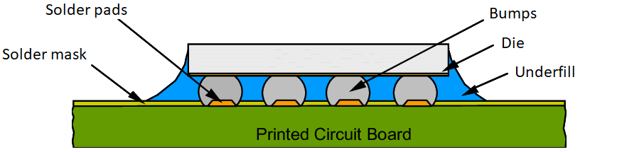
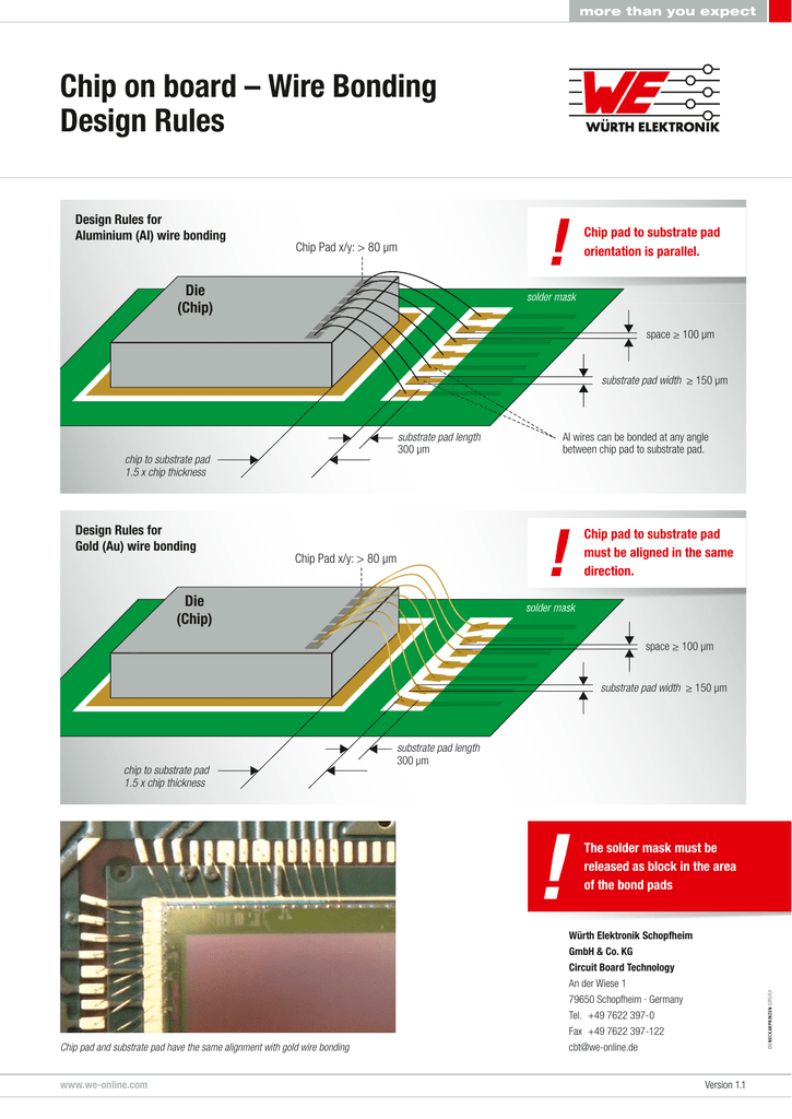
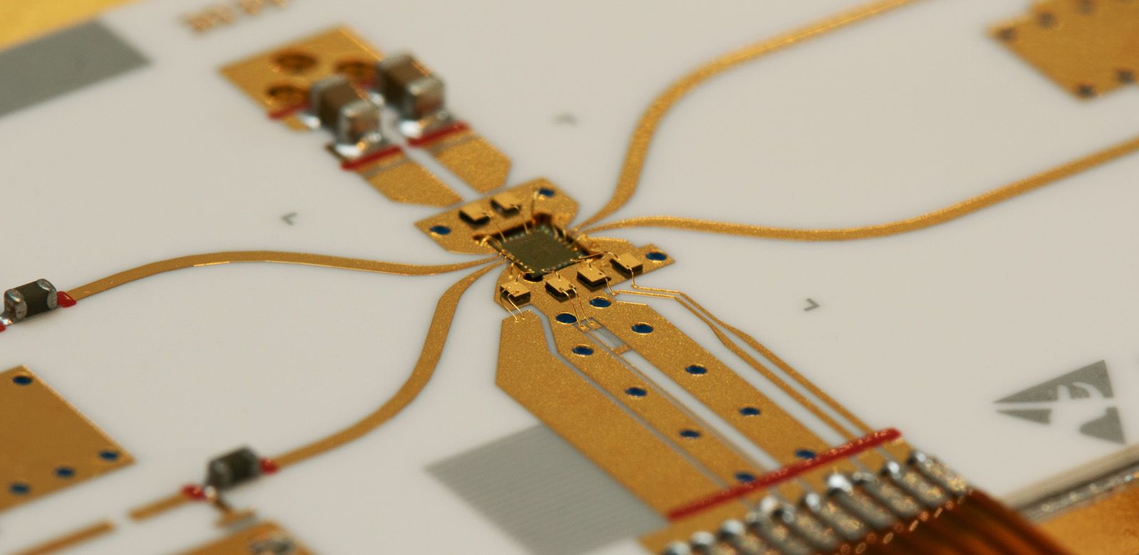
PCB Design Rules for Chip-on-Board Layout

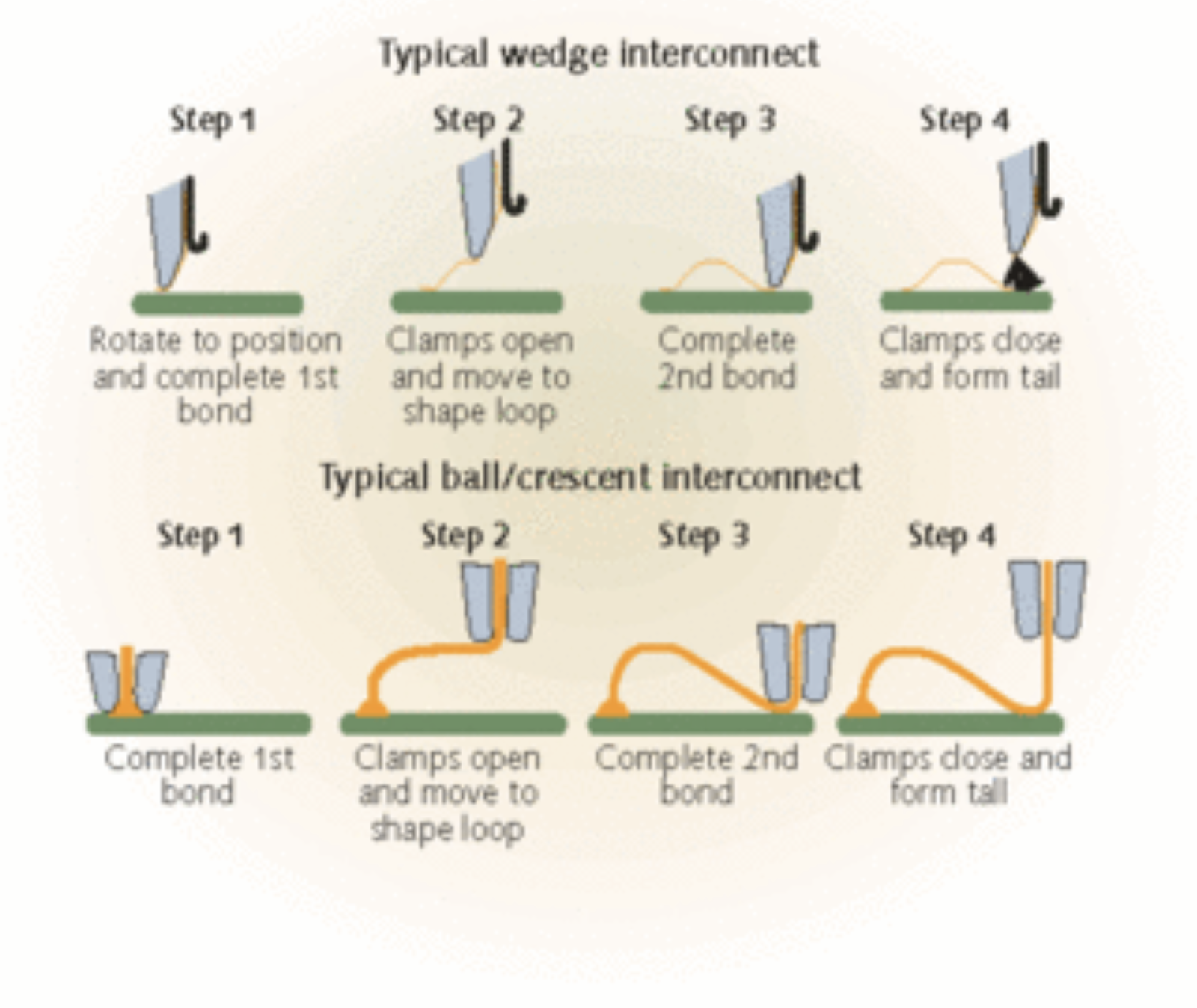
Wire Bonding - SK hynix Newsroom
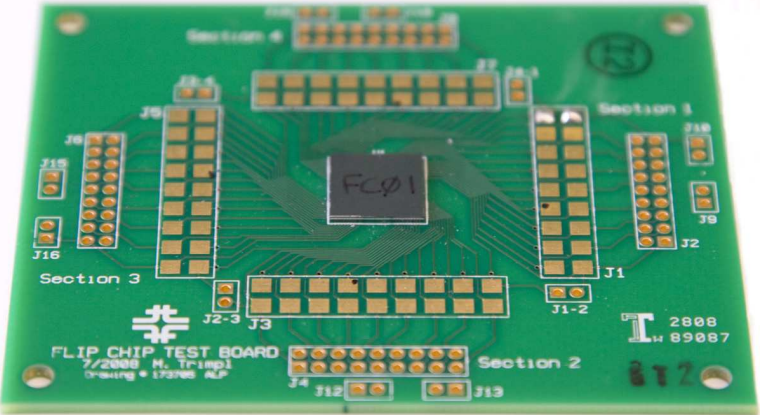
PCB Layout of Chips On Board - Skip the Package and Join the Fun

반도체 후공정 - SK hynix : 네이버 블로그
Wire Bonding, Advanced PCB Design Blog
PCB Design Rules for Chip-on-Board Layout

How is working bonding machine to weld chip IC to PCB.

반도체 특강] 와이어본딩(Wire Bonding), 칩을 바느질해 PCB에 연결하다 - Computing - 랩터 인터내셔널
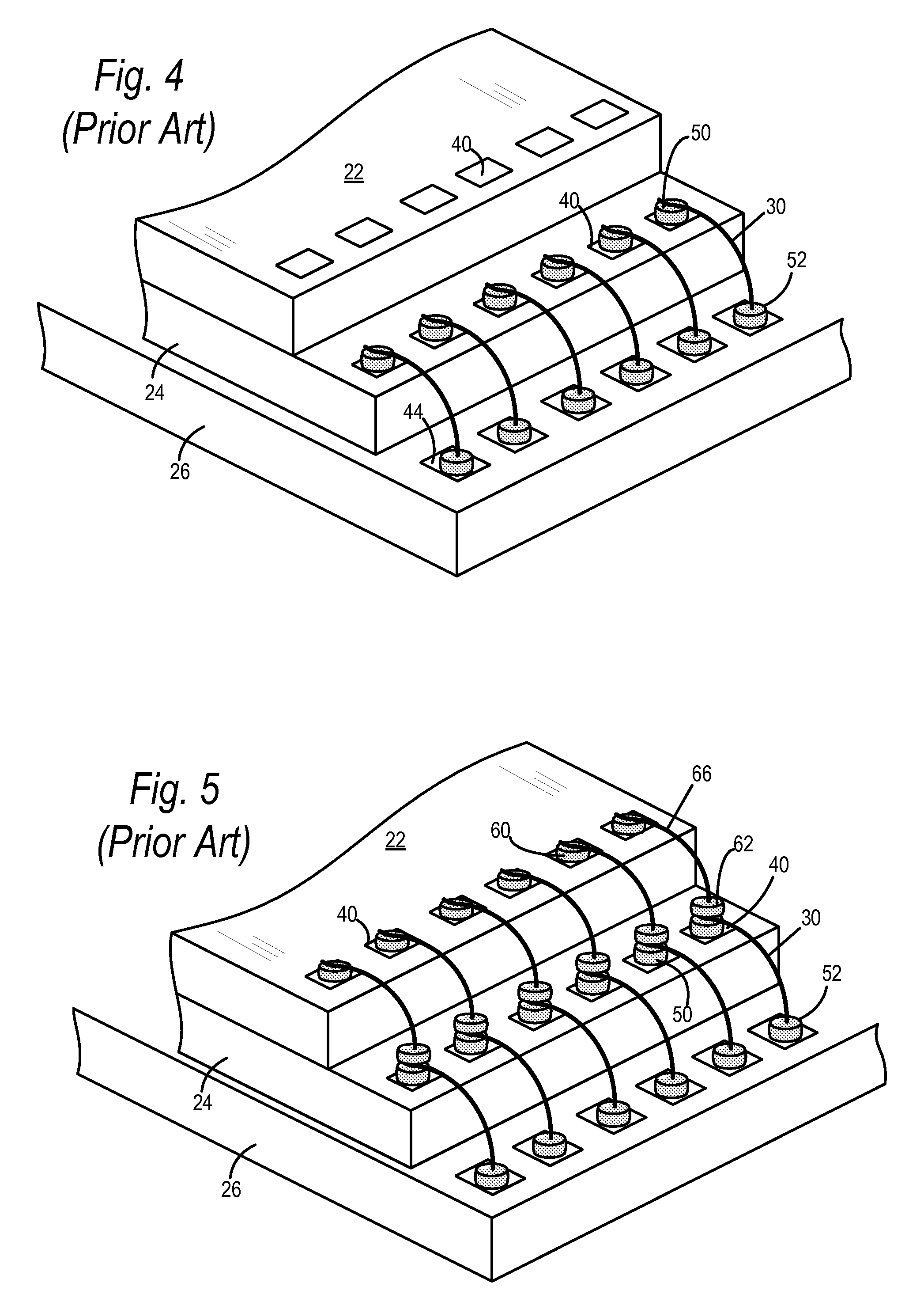
Wire on wire stitch bonding in a semiconductor device - Eureka

SK Hynix to invest $107bn in 4 new semiconductor plants
Eurotronics - Hybrid circuits